

 Click it and Unblock the Notifications
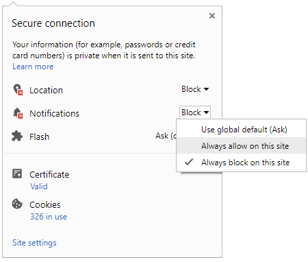
Nanowall 3D technology to give super touchscreen experience
In a first, a team of researchers has used 3D print technology to create a new type of transparent electrode to enhance the display quality and touchscreen experience. A research team led by Dimos Poulikakos, professor of thermodynamics at ETH University in Zurich, Switzerland, created a transparent electrode that takes the form of a grid made of gold or silver "nanowalls" on a glass surface.

The walls or electrodes, hardly be seen with the naked eye, have a higher conductivity and are more transparent than those made of indium tin oxide -- the standard material used in smartphones and tablets today - giving a better the screen quality and precision to the touchscreen.
SEE ALSO: How To Remotely Locate And Erase Data on-Your Windows 10 Smartphone
"Indium tin oxide is used because the material has a relatively high degree of transparency and the production of thin layers has been well researched, but it is only moderately conductive," said Patrik Rohner, a PhD student in Poulikakos' team.
In order to produce more conductive electrodes, the team opted for gold and silver, which conduct electricity much better. Since these metals are not transparent, the scientists had to make use of the third dimension.
"If you want to achieve both high conductivity and transparency in wires made from these metals, you have a conflict of objectives. As the cross-sectional area of gold and silver wires grows, the conductivity increases, but the grid's transparency decreases," Poulikakos said.
SEE ALSO: Top 10 Smartphones, priced Under Rs 10,000
To make the plan work, the team used metal walls only 80 to 500 nanometres thick. Since the walls are two to four times taller than they are wide, the cross-sectional area, and thus the conductivity, was found sufficiently high. The researchers used printing process known as Nanodrip to produce these tiny metal walls.
Nanodrip, that Poulikakos and his colleagues developed three years ago, is a process in which they used inks made from metal nanoparticles in a solvent. An electrical field draws ultra-small droplets of the metallic ink out of a glass capillary. The solvent evaporates quickly, allowing a three-dimensional structure to be built up drop by drop. The paper was published in the journal International Business Times.
Source IANS
-
 54,999
 -
 99,999
 -
 1,44,900
 -
 89,998
 -
 46,500
 -
 57,998
 -
 53,989
 -
 1,59,999
 -
 1,29,999
 -
 99,999
-
 70,499
 -
 1,56,900
 -
 1,30,990
 -
 17,084
 -
 16,999
 -
 30,999
 -
 9,999
9,999 -
 79,900
 -
 8,999
8,999 -
 79,999
-
 20,999
 -
 37,999
 -
 25,999
 -
 31,999
 -
 24,999
 -
 10,999
 -
 15,999
 -
 45,999
 -
 19,499
 -
 1,61,999