

 Click it and Unblock the Notifications
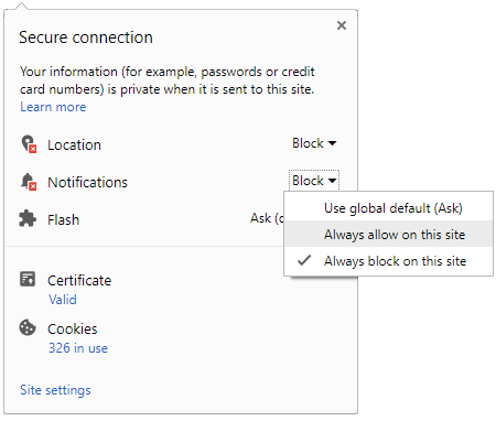
Intel Shows Off Future of Chipmaking With 18A-P and Beyond-GAA Research
Intel Foundry has provided an update on its process technology roadmap, revealing significant manufacturing milestones and long-term research initiatives. The company announced that Intel 18A-P, the first performance-focused evolution of the Intel 18A process family, has entered risk production. The achievement aligns with the deployment timeline previously shared with customers and underscores Intel's commitment to delivering advanced semiconductor technologies.
Naga Chandrasekaran, Executive Vice President at Intel Foundry, stated that the latest disclosures demonstrate the company's dedication to leading-edge process innovation. While acknowledging the engineering challenges that remain, he emphasized Intel's continued investment in long-range research and development.

Technical Performance and Transistor Enhancements
The Intel 18A-P process introduces several improvements in power efficiency, performance, and design flexibility through the co-optimization of transistors, interconnects, and design technologies.
Key enhancements include:
- Up to 9% higher performance at the same power level compared to Intel 18A.
- Up to 18% lower power consumption at equivalent performance levels.
- Introduction of Power Boost, a dual-contact low-resistance transistor option that increases drive current and enables higher operating frequencies.
- 20%-40% reduction in thermal resistance through advanced materials and design innovations.
- 10%-30% lower vertical via resistance achieved through geometry and material optimizations.
- PMOS via strain engineering to improve carrier mobility and transistor efficiency.
New low-power and high-performance transistor options, along with a fifth logic threshold voltage pair for greater design flexibility.
Intel 18A-P maintains full design-rule compatibility with the standard Intel 18A process, allowing chipmakers to reuse existing intellectual property and design flows. The node also retains key specifications, including 180nm and 160nm cell heights and a 50nm contacted poly pitch.
Silicon Validation and Advanced Architecture
During the symposium, Intel showcased the benefits of its gate-all-around (GAA) transistor architecture and backside power delivery (BSPD) technology, both commercialized with the Intel 18A node. According to Eric Karl, Vice President and Fellow at Intel Foundry, these innovations provide an 11% reduction in routed area and a tenfold reduction in dynamic voltage droop. The improvements can deliver up to a 6% frequency increase or more than 15% dynamic power savings compared to conventional frontside interconnect approaches.
Manju Shamanna from Intel's Silicon Engineering group also presented silicon validation results from CPU cores utilizing GAA and BSPD technologies. The data showed improved frequency scaling at lower voltages, including approximately 30% higher frequency operation at 0.5V while reducing IR drop and maintaining efficiency.
Long-Term Silicon Scaling Research
Looking beyond current-generation technologies, Intel unveiled several research projects aimed at extending silicon scaling beyond gate-all-around architectures. The company demonstrated monolithic complementary field-effect transistor (CFET) inverters featuring vertically stacked NMOS and PMOS devices at a 45nm gate pitch.
Intel also showcased the integration of gallium nitride (GaN) power devices with conventional silicon logic on 300mm wafers. The demonstration included a 1,000-gate digital control block integrated alongside high-performance power components on a single die.
Additionally, Intel highlighted progress in subtractive ruthenium interconnect technology with air-gap integration, which achieved up to a 35% reduction in capacitance compared to copper-based interconnects, providing a promising path for future semiconductor scaling.
-
 1,29,999
 -
 22,999
 -
 64,999
 -
 99,999
 -
 29,999
 -
 39,999
 -
-
 63,999
 -
 1,56,900
 -
 96,949

-
 1,39,900
 -
 1,29,900
 -
 79,900
 -
 65,900
 -
 12,999
 -
96,949
-
 16,499
 -
 38,999
 -
 30,700
 -
 49,999
-
 19,999
 -
 17,970
 -
 21,999
 -
 13,474
 -
 18,999
 -
 22,999
 -
 19,999
 -
 17,999
 -
 26,999
 -
 5,999
5,999